(United Kingdom)

Product Summary
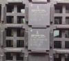
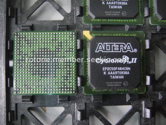
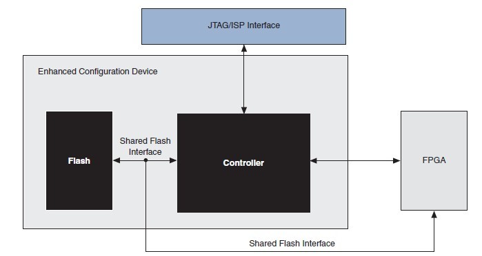
The Altera enhanced configuration device EP2C50F484C6N is a single-device, high-speed, advanced configuration solution for very high-density FPGAs. The core of an enhanced configuration device is divided into two major blocks: a confguration controller and a flash memory. The flash memory of EP2C50F484C6N is used to store configuration data for systems made up of one or more Altera FPGAs. Unused portions of the flash memory can be used to store processor code or data that can be accessed via the external flash interface after FPGA configuration is complete.
Parametrics
EP2C50F484C6N absolute maximum ratings: (1)VCC Supply voltage With respect to ground: -0.2 to 4.6 V; (2)VI DC input voltage With respect to ground: -0.5 to 3.6 V; (3)IMAX DC VCC or ground current: 100 mA; (4)IOUT DC output current, per pin: -25 to 25 mA; (5)PD Power dissipation: 360 mW; (6)TSTG Storage temperature: -65 to 150℃; (7)TAMB Ambient temperature: -65 to 135℃; (8)TJ Junction temperature: 135℃.
Features
EP2C50F484C6N features: (1)Standard flash die and a controller die combined into single stacked chip package; (2)External flash interface supports parallel programming of flash and external processor access to unused portions of memory; (3)Flash memory block/sector protection capability via external flash interface; (4)Supported in EPC16 and EPC4 devices; (5)Page mode support for remote and local reconfiguration with up to eight configurations for the entire system; (6)Compatible with Stratix series Remote System Configuration feature; (7)Supports byte-wide configuration mode fast passive parallel (FPP); 8-bit data output per DCLK cycle; (8)Supports true n-bit concurrent configuration (n = 1, 2, 4, and 8) of Altera FPGAs; (9)Pin-selectable 2-ms or 100-ms power-on reset (POR) time; (10)Configuration clock supports programmable input source and frequency synthesis; (11)Multiple configuration clock sources supported (internal oscillator and external clock input pin); (12)External clock source with frequencies up to 100 MHz; (13)Internal oscillator defaults to 10 MHz; Programmable for higher frequencies of 33, 50, and 66 MHz; (14)Clock synthesis supported via user programmable divide counter; (15)Available in the 100-pin plastic quad flat pack (PQFP) and the 88-pin Ultra FineLine BGAR (UFBGA) packages; (16)Vertical migration between all devices supported in the 100-pin PQFP package; (17)Supply voltage of 3.3 V (core and I/O); (18)Hardware compliant with IEEE Std. 1532 in-system programmability (ISP) specification; (19)Supports ISP via Jam Standard Test and Programming Language (STAPL); (20)Supports JTAG boundary scan; (21)nINIT_CONF pin allows private JTAG instruction to start FPGA configuration; (22)Internal pull-up resistor on nINIT_CONF always enabled; (23)User programmable weak internal pull-up resistors on nCS and OE pins; (24)Internal weak pull-up resistors on external flash interface address and control lines, bus hold on data lines; (25)Standby mode with reduced power consumption.
Diagrams
| Image | Part No | Mfg | Description |  |
Pricing (USD) |
Quantity | ||||||
|---|---|---|---|---|---|---|---|---|---|---|---|---|
 |
 EP2C50F484C6N |
|
IC CYCLONE II FPGA 50K 484-FBGA |
Data Sheet |
|
|
||||||
| Image | Part No | Mfg | Description | |
Pricing (USD) |
Quantity | ||||||
 |
EP2C15AF256C6N |
|
IC CYCLONE II FPGA 15K 256-FBGA |
Data Sheet |
|
|
||||||
|
EP2C15AF256C7N |
|
IC CYCLONE II FPGA 15K 256-FBGA |
Data Sheet |
|
|
||||||
|
EP2C15AF256C8N |
|
IC CYCLONE II FPGA 15K 256-FBGA |
Data Sheet |
|
|
||||||
|
EP2C15AF256I8N |
|
IC CYCLONE II FPGA 15K 256-FBGA |
Data Sheet |
|
|
||||||
|
EP2C15AF484C6N |
|
IC CYCLONE II FPGA 15K 484-FBGA |
Data Sheet |
|
|
||||||
|
EP2C15AF484C7N |
|
IC CYCLONE II FPGA 15K 484-FBGA |
Data Sheet |
|
|
||||||